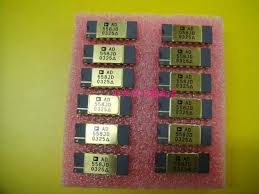
AD558SD
The AD558has been configured for ease of /application. All eference,
output amplifier and logic connections are made internally.
In addition, all calibration trims are performed at the
factory assuring specified accuracy without user trims. The only
connection decision that must be made by the user is a single
jumper to select output voltage range. Clean circuit board layout
is facilitated by isolating all digital bit inputs on one side of
The high speed output buffer amplifier is operated in the non-
inverting mode with gain determined by the user-connections
at the output range select pin. The gain-setting application
resistors are thin-film laser-trimmed to match and track the
DAC resistors and to assure precise initial calibration of the two
output ranges, 0 V to 2.56 V and 0 V to 10 V. The amplifier
output stage is an NPN transistor with passive pull-down for
zero-based output capability with a single power supply. The
internal precision voltage reference is of the patented bandgap
type. This design produces a reference voltage of 1.2 volts and
thus, unlike 6.3 volt temperature compensated Zeners, may be
operated from a single, low voltage logic power supply. The
microprocessor interface logic consists of an 8-bit data latch and
control circuitry. Low power, small geometry and high speed
are advantages of the I2L design as applied to this section. I2L is
the package; analog outputs are on the opposite side.
Figure 3 shows the two alternative output range connections.
The 0 V to 2.56 V range may be selected for use with any power
supply between +4.5 V and +16.5 V. The 0 V to 10 V range
requires a power supply of +11.4 V to +16.5 V.

- موجود در انبار : 10
- قیمت : 100,000 تومان
- برچسب ها : The AD558has been configured for ease of /application. All eference ، output amplifier and logic connections are made internally. In addition ، all calibration trims are performed at the factory assuring specified accuracy without user trims. The only connection decision that must be made by the user is a single jumper to select output voltage range
درحال بارگزاری
درحال بارگزاری
درحال بارگزاری
 سبد خرید
 ورود به حساب من
 سفارش من


